- 您现在的位置:买卖IC网 > Sheet目录346 > NCP692MN50T2GEVB (ON Semiconductor)EVAL BOARD FOR NCP692MN50T2G
�� �
�
�NCP690,� NCP691,� NCP692,� NCV8690�
�divider� network� as� shown� on� Figure� 4.� The� output� voltage�
�and� resistors� should� be� chosen� using� Equations� 1� and� 2.�
�The� power� dissipated� by� the� NCP690� can� be� calculated�
�from� the� following� equations:�
�V� OUT� +� 1.250� 1� )�
�R� 1�
�R� 2�
�)� (I� ADJ� @� R� 1� )�
�(eq.� 1)�
�or�
�P� D� [� V� IN� (I� GND� @I� OUT� )� )� I� OUT� (V� IN� *� V� OUT� )�
�(eq.� 4)�
�R� 2� ^� R� 1�
�1�
�V� OUT�
�1.25�
�*� 1�
�(eq.� 2)�
�V� IN(MAX)� [�
�P� D(MAX)� )� (V� OUT�
�I� OUT� )� I� GND�
�I� OUT� )�
�(eq.� 5)�
�Input� bias� current� I� ADJ� is� typically� less� than� 210� nA.�
�Choose� R� 1� arbitrarily� to� minimize� errors� due� to� the� bias�
�current� and� to� minimize� noise� contribution� to� the� output�
�voltage.� Use� Equation� 2� to� find� the� required� value� for� R� 2� .� If�
�an� output� voltage� of� 1.25� V� is� desired,� the� adjustable� pin�
�250�
�200�
�should� be� connected� directly� to� the� output� pin.�
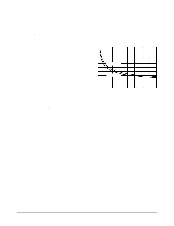
�Thermal� Characteristics�
�As� power� dissipated� in� the� NCP690� increases,� it� might�
�become� necessary� to� provide� some� thermal� relief.� The�
�maximum� power� dissipation� supported� by� the� device� is�
�dependent� upon� board� design� and� layout.� Mounting� pad�
�configuration� on� the� PCB,� the� board� material,� and� the�
�150�
�100�
�50�
�FR4� ?� 1.0 oz�
�FR4� ?� 2.0 oz�
�ambient� temperature� affect� the� rate� of� junction� temperature�
�rise� for� the� part.� When� the� NCP690� has� good� thermal�
�conductivity� through� the� PCB,� the� junction� temperature� will�
�be� relatively� low� with� high� power� applications.� The�
�0�
�0� 200� 400� 600�
�COPPER� AREA� (mm� 2� )�
�Figure� 32.� Thermal� Resistance� vs.� Copper� Area�
�800�
�R� q� JA�
�maximum� dissipation� the� NCP690� can� handle� is� given� by:�
�[T� J(MAX)� *� T� A� ]�
�P� D(MAX)� +� (eq.� 3)�
�Since� T� J� is� not� recommended� to� exceed� 125� °� C� (T� J(MAX)� ),�
�then� the� NCP690� can� dissipate� up� to� 1� W� when� the� ambient�
�temperature� (T� A� )� is� 25� °� C.�
�Hints�
�V� IN� and� GND� printed� circuit� board� traces� should� be� as�
�wide� as� possible.� When� the� impedance� of� these� traces� is�
�high,� there� is� a� chance� to� pick� up� noise� or� cause� the� regulator�
�to� malfunction.� Place� external� components,� especially� the�
�output� capacitor,� as� close� as� possible� to� the� NCP690,� and�
�make� traces� as� short� as� possible.�
�http://onsemi.com�
�12�
�发布紧急采购,3分钟左右您将得到回复。
相关PDF资料
NCV7513AFTR2G
IC PREDRIVER HEX LOW SIDE 32LQFP
NCV7513BFTR2G
IC PREDRIVER HEX LOW SIDE 32LQFP
NCV7513FTG
IC PREDRIVER HEX LOSIDE 32-LQFP
NCV7517BFTR2G
IC PREDRIVER HEX LOW SIDE 32LQFP
NCV8855BMNR2GEVB
BOARD EVALUATION NCV8855 ASIC
NCV8871BSTGEVB
BOARD EVAL NCV8871BST BOOST CTLR
NHC-14150
VALULINE 8" X 8.5" X 1.75"
NHC-14151
VALULINE 8" X 17" X 1.75"
相关代理商/技术参数
NCP692MNADJT2G
功能描述:低压差稳压器 - LDO LDO RoHS:否 制造商:Texas Instruments 最大输入电压:36 V 输出电压:1.4 V to 20.5 V 回动电压(最大值):307 mV 输出电流:1 A 负载调节:0.3 % 输出端数量: 输出类型:Fixed 最大工作温度:+ 125 C 安装风格:SMD/SMT 封装 / 箱体:VQFN-20
NCP692MNADT2GEVB
功能描述:BOARD EVAL NCP692 ADJ RoHS:是 类别:编程器,开发系统 >> 评估板 - 线性稳压器 (LDO) 系列:* 产品变化通告:1Q2012 Discontinuation 30/Mar/2012 设计资源:NCP590MNDPTAGEVB Gerber Files 标准包装:1 系列:- 每 IC 通道数:2 - 双 输出电压:1.8V,2.8V 电流 - 输出:300mA 输入电压:2.1 ~ 5.5 V 稳压器类型:正,固定式 工作温度:-40°C ~ 85°C 板类型:完全填充 已供物品:板 已用 IC / 零件:NCP590MNDP 其它名称:NCP590MNDPTAGEVB-NDNCP590MNDPTAGEVBOS
NCP693
制造商:ONSEMI 制造商全称:ON Semiconductor 功能描述:1A CMOS Low-Dropout Voltage Regulator
NCP693DMN08TCG
功能描述:低压差稳压器 - LDO 1A CMOS Low-Dropout Volt Regulator RoHS:否 制造商:Texas Instruments 最大输入电压:36 V 输出电压:1.4 V to 20.5 V 回动电压(最大值):307 mV 输出电流:1 A 负载调节:0.3 % 输出端数量: 输出类型:Fixed 最大工作温度:+ 125 C 安装风格:SMD/SMT 封装 / 箱体:VQFN-20
NCP693DMN10TCG
功能描述:低压差稳压器 - LDO 1A CMOS Low-Dropout Voltage Regulator RoHS:否 制造商:Texas Instruments 最大输入电压:36 V 输出电压:1.4 V to 20.5 V 回动电压(最大值):307 mV 输出电流:1 A 负载调节:0.3 % 输出端数量: 输出类型:Fixed 最大工作温度:+ 125 C 安装风格:SMD/SMT 封装 / 箱体:VQFN-20
NCP693DMN12TCG
功能描述:低压差稳压器 - LDO 1A CMOS Low-Dropout Volt Regulator RoHS:否 制造商:Texas Instruments 最大输入电压:36 V 输出电压:1.4 V to 20.5 V 回动电压(最大值):307 mV 输出电流:1 A 负载调节:0.3 % 输出端数量: 输出类型:Fixed 最大工作温度:+ 125 C 安装风格:SMD/SMT 封装 / 箱体:VQFN-20
NCP693DMN25TCG
功能描述:低压差稳压器 - LDO 1A CMOS Low-Dropout Volt Regulator RoHS:否 制造商:Texas Instruments 最大输入电压:36 V 输出电压:1.4 V to 20.5 V 回动电压(最大值):307 mV 输出电流:1 A 负载调节:0.3 % 输出端数量: 输出类型:Fixed 最大工作温度:+ 125 C 安装风格:SMD/SMT 封装 / 箱体:VQFN-20
NCP693DMN33TCG
功能描述:低压差稳压器 - LDO 1A CMOS Low-Dropout Volt Regulator RoHS:否 制造商:Texas Instruments 最大输入电压:36 V 输出电压:1.4 V to 20.5 V 回动电压(最大值):307 mV 输出电流:1 A 负载调节:0.3 % 输出端数量: 输出类型:Fixed 最大工作温度:+ 125 C 安装风格:SMD/SMT 封装 / 箱体:VQFN-20